Difference between revisions of "SOEDGE"
(Outsourced information) |
|||
| (9 intermediate revisions by the same user not shown) | |||
| Line 1: | Line 1: | ||
[[File:SOEdge.png|400px|thumb|right|The SOEDGE]] | [[File:SOEdge.png|400px|thumb|right|The SOEDGE]] | ||
The '''SOEDGE''' is a 3TOPS compute module that can be paired with the [[SOEDGE Baseboard]] or USB 3.0 and PCIe adapters for development. It can connect to a SBC, such as the ROCKPro64 or a regular PC. | The '''SOEDGE''' is a 3TOPS compute module that can be paired with the [[SOEDGE Baseboard]], the [[Clusterboard]] or USB 3.0 and PCIe adapters for development. It can connect to a SBC, such as the ROCKPro64 or a regular PC. | ||
== Software releases == | == Software releases == | ||
| Line 8: | Line 8: | ||
== SoC and Memory Specification == | == SoC and Memory Specification == | ||
[[File:RK1808_icon.png|right]] | [[File:RK1808_icon.png|right]] | ||
Based on the [https://www.rock-chips.com/a/en/products/RK18_Series/2019/0529/989.html Rockchip RK1808]. | |||
=== CPU Architecture === | === CPU Architecture === | ||
| Line 28: | Line 29: | ||
=== Neural Process Unit NPU Capability === | === Neural Process Unit NPU Capability === | ||
[[File:Vivante_Acuity_SDK.jpg|right|400px]] | |||
* [https://www.verisilicon.com/en/IPPortfolio/VivanteNPUIP NPU IP from Verisilicon Vivante] | * [https://www.verisilicon.com/en/IPPortfolio/VivanteNPUIP NPU IP from Verisilicon Vivante] | ||
* Support max 1920 Int8 MAC operation per cycle | * Support max 1920 Int8 MAC operation per cycle | ||
| Line 35: | Line 38: | ||
* One isolated voltage domain to support DVFS | * One isolated voltage domain to support DVFS | ||
* [https://github.com/VeriSilicon/acuity-models Acuity models Github] | * [https://github.com/VeriSilicon/acuity-models Acuity models Github] | ||
=== System Memory === | === System Memory === | ||
| Line 44: | Line 45: | ||
== Schematics and certifications == | == Schematics and certifications == | ||
SOEDGE module schematics: | SOEDGE module schematics: | ||
* [https://files.pine64.org/doc/SOEdge/SOEdge-Schematic-v2.0-190919.pdf SOEDGE Module ver 2.0 20190919 Schematic] | |||
* [https://files.pine64.org/doc/SOEdge/SoEdge-PCB-placement-v2.0-topplace.pdf SOEDGE Module ver 2.0 20190919 PCB Component Placement Top PDF file] | |||
* [https://files.pine64.org/doc/SOEdge/SoEdge-PCB-placement-v2.0-bottomplace.pdf SOEDGE Module ver 2.0 20190919 PCB Component Placement Bottom PDF file] | |||
* [https://files.pine64.org/doc/SOEdge/SoEdge-PCB-placement-v2.0-topplace.dxf SOEDGE Module ver 2.0 20190919 PCB Component Placement Top Drawing file] | |||
* [https://files.pine64.org/doc/SOEdge/SoEdge-PCB-placement-v2.0-bottomplace.dxf SOEDGE Module ver 2.0 20190919 PCB Component Placement Bottom Drawing file] | |||
* [https://files.pine64.org/doc/SOEdge/SOEdge%20Pin%20Assignments%20ver%201.00.xlsx SOEDGE Module Pin Assignment ver 1.0 in Excel format(includes comparison chart to SOPine)] | |||
* [https://files.pine64.org/doc/SOEdge/SOEdge%20Pin%20Assignments%20ver%201.00.ods SOEDGE Module Pin Assignment ver 1.0 in Open Document format(includes comparison chart to SOPine)] | |||
SOEDGE Neural AI Stick schematic: | SOEDGE Neural AI Stick schematic: | ||
| Line 63: | Line 64: | ||
== Datasheets for Components and Peripherals == | == Datasheets for Components and Peripherals == | ||
Rockchip RK1808 SoC information: | |||
* [http://opensource.rock-chips.com/images/4/43/Rockchip_RK1808_Datasheet_V1.2_20190527.pdf Rockchip RK1808 ver 1.2 datasheet] | |||
* [https://files.pine64.org/doc/datasheet/SOEdge/Rockchip%20RK1808%20TRM%20Part1%20V1.2--20190826%20open%20source.pdf Rockchip TK1808 Technical Reference Manual Part 1] | |||
Rockchip RK809 PMU (Power Management Unit) information: | |||
* [https://rockchip.fr/RK809%20datasheet%20V1.01.pdf Rockchip RK809 PMIC Datasheet] | |||
DDR4 information: | |||
* [https://files.pine64.org/doc/datasheet/SOEdge/Micron%208Gb_DDR4_SDRAM.pdf Micron DDR4 Datasheet] | |||
eMMC information: | |||
* [https://files.pine64.org/doc/rock64/PINE64_eMMC_Module_20170719.pdf PINE64 eMMC module schematic] | |||
* [https://files.pine64.org/doc/rock64/usb%20emmc%20module%20adapter%20v2.pdf PINE64 USB adapter for eMMC module V2 schematic] | |||
* [https://files.pine64.org/doc/rock64/USB%20adapter%20for%20eMMC%20module%20PCB.tar PINE64 USB adapter for eMMC module PCB in JPEG] | |||
* [https://files.pine64.org/doc/datasheet/pine64/E-00517%20FORESEE_eMMC_NCEMAM8B-16G%20SPEC.pdf 16GB Foresee eMMC Datasheet] | |||
* [https://files.pine64.org/doc/datasheet/pine64/SDINADF4-16-128GB-H%20data%20sheet%20v1.13.pdf 32GB/64GB/128GB SanDisk eMMC Datasheet] | |||
SPI NOR Flash information: | |||
* [https://files.pine64.org/doc/datasheet/pine64/w25q128jv%20spi%20revc%2011162016.pdf WinBond 128Mb SPI Flash Datasheet] | |||
* [https://files.pine64.org/doc/datasheet/pine64/GD25Q128C-Rev2.5.pdf GigaDevice 128Mb SPI Flash Datasheet] | |||
SOEDGE Related: | SOEDGE Related: | ||
| Line 98: | Line 103: | ||
** [https://files.pine64.org/doc/datasheet/pine64/0.5FPC%20Front%20Open%20Connector%20H=1.5.pdf 0.5mm Pitch cover type FPC connector specification use in DSI port, TP port and CSI port] | ** [https://files.pine64.org/doc/datasheet/pine64/0.5FPC%20Front%20Open%20Connector%20H=1.5.pdf 0.5mm Pitch cover type FPC connector specification use in DSI port, TP port and CSI port] | ||
= Debugging = | == Debugging == | ||
== Serial Console == | === Serial Console === | ||
System Serial is located on PI-5 bus (11x2 GPIO header). | System Serial is located on PI-5 bus (11x2 GPIO header). | ||
| Line 107: | Line 112: | ||
* GND: Pin 10 (Black cable) (Connect to GND on Serial adapter) | * GND: Pin 10 (Black cable) (Connect to GND on Serial adapter) | ||
[[File:Soedge_serial_pins.jpg]] | [[File:Soedge_serial_pins.jpg|400px]] | ||
The default baudrate is 1500000, note that not all serial adapters support this high baudrate. | The default baudrate is 1500000, note that not all serial adapters support this high baudrate. | ||
[[Category:SOEDGE]] [[Category:Rockchip RK1808]] | [[Category:SOEDGE]] [[Category:Rockchip RK1808]] | ||
Latest revision as of 08:41, 12 April 2023
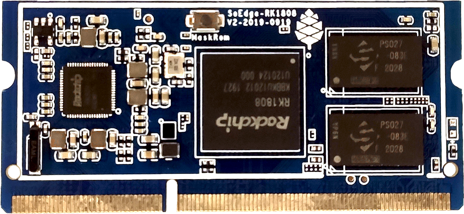
The SOEDGE is a 3TOPS compute module that can be paired with the SOEDGE Baseboard, the Clusterboard or USB 3.0 and PCIe adapters for development. It can connect to a SBC, such as the ROCKPro64 or a regular PC.
Software releases
The SOEDGE software releases can be found in the article SOEDGE Software Releases.
SoC and Memory Specification
Based on the Rockchip RK1808.
CPU Architecture
- Dual-core ARM Cortex-A35 Processor@1600-2000Mhz
- A power-efficient ARM 64-Bit Armv8-A architecture
- AArch32 for full backward compatibility with Armv7
- Support NEON Advanced SIMD (Single Instruction Multiple Data) instruction for acceleration of media and signal processing function
- Support Large Physical Address Extensions(LPAE)
- VFPv4 Floating Point Unit
- 32KB L1 Instruction cache and 32KB L1 Data cache
- AArch64 for 64-bit support and new architectural features
- TrustZone security technology
- Neon Advanced SIMD
- DSP and SIMD extensions
- VFPv4 Floating point
- Hardware virtualization support
- 128KB L2 cache
Neural Process Unit NPU Capability
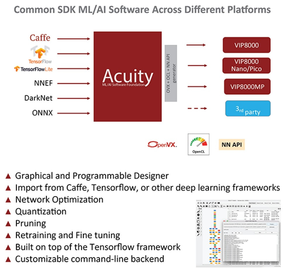
- NPU IP from Verisilicon Vivante
- Support max 1920 Int8 MAC operation per cycle
- Support max192 Int16 MAC operation per cycle
- Support max 64 FP16 MAC operation per cycle
- 512KB internal buffer
- One isolated voltage domain to support DVFS
- Acuity models Github
System Memory
- RAM Memory Variants: 2GB DDR4.
- Storage Memory: 128Mb SPI Flash and optional eMMC module from 16GB up to 128GB
Schematics and certifications
SOEDGE module schematics:
- SOEDGE Module ver 2.0 20190919 Schematic
- SOEDGE Module ver 2.0 20190919 PCB Component Placement Top PDF file
- SOEDGE Module ver 2.0 20190919 PCB Component Placement Bottom PDF file
- SOEDGE Module ver 2.0 20190919 PCB Component Placement Top Drawing file
- SOEDGE Module ver 2.0 20190919 PCB Component Placement Bottom Drawing file
- SOEDGE Module Pin Assignment ver 1.0 in Excel format(includes comparison chart to SOPine)
- SOEDGE Module Pin Assignment ver 1.0 in Open Document format(includes comparison chart to SOPine)
SOEDGE Neural AI Stick schematic:
SOEDGE/SOPINE/PINE A64 WiFi/BT module schematics:
SOEDGE module together with the baseboard certification:
- Disclaimer: Please note that SOEDGE module is not a "final" product and in general certification is not necessary. However, SOEDGE module still submits the mpdel A baseboard for FCC, CE, and ROHS certifications and obtain the certificates to prove that can pass the testing. Please note, a final commercial product needs to perform its own testing and obtain its own certificate.
- Not yet available
Datasheets for Components and Peripherals
Rockchip RK1808 SoC information:
Rockchip RK809 PMU (Power Management Unit) information:
DDR4 information:
eMMC information:
- PINE64 eMMC module schematic
- PINE64 USB adapter for eMMC module V2 schematic
- PINE64 USB adapter for eMMC module PCB in JPEG
- 16GB Foresee eMMC Datasheet
- 32GB/64GB/128GB SanDisk eMMC Datasheet
SPI NOR Flash information:
SOEDGE Related:
- LCD Touch Screen Panel information:
- Ethernet PHY information:
- Wifi/BT module information:
- Enclosure information:
- Connector information:
Debugging
Serial Console
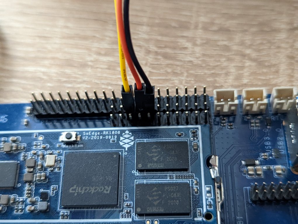
System Serial is located on PI-5 bus (11x2 GPIO header).
- TXD: Pin 6 (Yellow cable) (Connect to RXD on Serial adapter)
- RXD: Pin 8 (Orange cable) (Connect to TXD on Serial adapter)
- GND: Pin 10 (Black cable) (Connect to GND on Serial adapter)
The default baudrate is 1500000, note that not all serial adapters support this high baudrate.


