Difference between revisions of "PinePhone v1.1 - Braveheart"
(add investigations, hacky fix) |
|||
| Line 18: | Line 18: | ||
# Add R630 resistor location, populate with 0K by default. Allows adjusting to different battery thermistors in case this is not possible in software. | # Add R630 resistor location, populate with 0K by default. Allows adjusting to different battery thermistors in case this is not possible in software. | ||
# Add voltage shift to Pogo pins I2C-CLK, I2C-DATA, and INT. The Pogo Pin specified voltage is 3.3v while the A64's I2C is 2.8V. | # Add voltage shift to Pogo pins I2C-CLK, I2C-DATA, and INT. The Pogo Pin specified voltage is 3.3v while the A64's I2C is 2.8V. | ||
# A64 LINEOUTN is disconnected from the speaker amplifier, making the speaker output single-ended instead of differential | |||
== Known issues == | == Known issues == | ||
| Line 131: | Line 132: | ||
I don't have a datasheet for the AW3512 chips, but I assume the enable input is active-high. VCONN1_EN and VCONN2_EN are open-drain. When they are open, it appears that VCONN should be enabled. But right now, when they are open, VCONN is disabled, because the AW3512 EN pin will be pulled low by the FET. | I don't have a datasheet for the AW3512 chips, but I assume the enable input is active-high. VCONN1_EN and VCONN2_EN are open-drain. When they are open, it appears that VCONN should be enabled. But right now, when they are open, VCONN is disabled, because the AW3512 EN pin will be pulled low by the FET. | ||
=== Speaker output could be differential === | |||
If a differential connection to the speaker amplifier doesn't cause any issues, using it would significantly lower the noise floor of the speaker, and would allow doubling the max volume. | |||
Revision as of 02:42, 17 February 2020
The PinePhone v1.1 "Braveheart" is a hardware revision of the PinePhone due to ship in January 2020.
This page contains resources which are exclusive to the 1.1 revision of the PinePhone. For other revisions, or for resources related to all PinePhone revisions, see PinePhone.
Schematic
Changes from 1.0
Braveheart is slightly different from the 1.0 revision of the Pinephone. These differences should not require creating different images.
- Added CPU shielding and cover plate
- Swap PC3 to FLASH_EN and PD24 to FLASH_TRIGOUT, where previously they were reversed
- Add pulldown resistor on PD24 (FLASH_TRIGOUT) so the flash LED does not light on boot
- Connect WiFi enable to VD33
- Set the EG25G's PWRKEY on by default (see resistor R1526)
- Add R630 resistor location, populate with 0K by default. Allows adjusting to different battery thermistors in case this is not possible in software.
- Add voltage shift to Pogo pins I2C-CLK, I2C-DATA, and INT. The Pogo Pin specified voltage is 3.3v while the A64's I2C is 2.8V.
- A64 LINEOUTN is disconnected from the speaker amplifier, making the speaker output single-ended instead of differential
Known issues
This section lists problems known on the 1.1 revision hardware, possibly because they carried over from the 1.0 revision.
Excess power consumption while using USB OTG
The N_VBUSEN/DRIVEVBUS input on the AXP803 PMIC, labeled USB-DRVVBUS on the schematic, is not connected to the USB OTG boost regulator enable input, because R1300 is marked "NC". This prevents the AXP803 from automatically detecting when the USB port is being powered from the battery. Thus, the PMIC continues to draw power from the USB port, and this doubles the drain on the battery (since the whole phone is being powered by the USB OTG boost regulator).
This could be fixed by populating R1300.
The ANX7688's VBUS_CTRL pin should also be connected to the DRVVBUS signal to perform role switching in hardware without needing OS interaction. In that case PD6 becomes an input. Otherwise, we would need to hook up the VBUS status change interrupt from the ANX7688 to control the USB PHY driver.
Modem Ring Indicator placement prevents deep sleep
The EG25G's Ring Indicator pin is currently routed to GPIO pin PB2.
Ring Indicator is a configurable signaling pin capable of notifying the modem's host of incoming messages or calls. This makes it important to read the status of the pin during (ARISC / Super Standby) sleep, since incoming calls or text messages must wake the device.
Using the PB bank of GPIO on the A64 requires VCC-IO to be switched on. DCDC1, which powers VCC-IO, also powers most of the rest of the phone, including the eMMC, microSD, and USB controller, and enables the POGO pins, WiFi, modem sound, motor, headphone port, etc.
The only GPIO bank that works (can receive interrupts) while the A64 is suspended, and is independent from the regulators powering other periphherals, is Port L (on R_PIO).
Modem AP_READY signal is not connected
The modem's power management documentation describes how to implement modem power saving. The modem can wake up the host using either the Ring Indicator pin (section 4.5) or USB remote wakeup (section 4.3). Either way, it suggests the AP_READY signal needs to be connected. The modem needs that signal to know when the host is asleep (and the modem needs to queue its messages and wake it up), and when the host has finished waking up (and is ready to receive the queued messages).
Ideally, when the modem is communicating over USB, it can use the USB host suspend state to know when the host is active, and would not need the separate AP_READY signal. It is not known whether this is the case.
Modem PWR_KEY signal is not connected
On dev phone (1.0) this signal was connected to PB3. This allows for turning on/off the modem via GPIO from a kernel driver. If proper power down is to be implemented in the kernel for the modem, to allow safe shutdown of the modem before turning off the 4g-pwr-bat, kernel has to be able to signal to the modem to shut down and wait 30s. This is not possible on braveheart. Without this signal, kernel can't do anyhting to shut down the modem, and would have to rely on userspace to properly manage the modem power up/down sequence. Relying on userspace risks users shutting down the modem without proper wait time of 30s, risking modem damage (flash data corruption).
It would be nice to also have access to the STATUS signal from the modem, so that the driver can detect whether the modem is on or off (userspace might have turned modem off already via AT commands). Given that PWR_KEY pulse will either turn the modem on or off, based on the current status, it's necessary to know the current status before sending the pulse.
There's a STATUS signal routed to PWR_KEY on BraveHeart, that keeps the PWRKEY deasserted when the modem is on and it's not possible to pull it up from PB3, even if R1516 would be optionally mounted. So after powerup you can't change PWR_KEY signal anymore from PB3 even if R1516 is mounted, and it's not possible to turn off the modem via PB3.
Modem UART flow control is broken
BB-TX and BB-RX are connected to UART3 (PD0/PD1). BB-RTS and BB-CTS are connected to UART4 (PD4/PD5). To use hardware flow control, TX/RX would need to be connected to UART4, swapping PD0/PD1 with the motor control and rear camera reset GPIOs at PD2/PD3. This would need a device tree change.
Hardware flow control can be disabled with the AT+IFC command, and USB can also be used for commands instead of the UART. So the impact of this problem is unclear.
Modem has access to sensors on I2C1
The modem is a master on the I2C1 bus. A malicious firmware on the modem would be able to read the phone's gravity/light/proximity sensors and prevent the main Linux OS from reading them. The modem's audio design note describes the AT+QIIC command which can be used to read and write registers on I2C devices.
According to the modem documentation, its I2C interface is only used for direct connection to a standalone audio codec. On the PinePhone, since the modem's audio is routed through the A64 SoC, the modem's I2C interface has no legitimate use.
The modem's I2C interface should be left floating. U1503 pins A1, A2, B1, and B2 can be disconnected, and R1527/R1528 can be removed.
WiFi module cannot be disabled in software
Neither the WL-REG-ON nor WL-PMU-EN signal is connected to anything, and the WiFi module's CHIP_EN pin is connected (through the killswitch) to a regulator that cannot be turned off (easily, if at all). So while the killswitch works, there's no way to disable the WiFi module in software. This will lead to excess power consumption when WiFi is turned off.
Magnetometer's IRQ signal is routed to the wrong pin
It needs to go to DRDY, not to INT. The kernel driver expects the trigger events to be fired when DRDY changes, and does not even configure the interrupts to be enabled on the INT pin.
Software workaround is to disable magnetometer interrupt in the devicetree, and use a hrtimer or some other software triggering mechanism for IIO devices.
Cameras have the same default I2C address
This makes it hard to keep both of them powered at the same time and switch quickly between them (on the per-frame basis) without having to re-initialize the sensors on each switch, which takes some time.
USB Power issue preventing charge and battery-less operation (one-off HW issue ?)
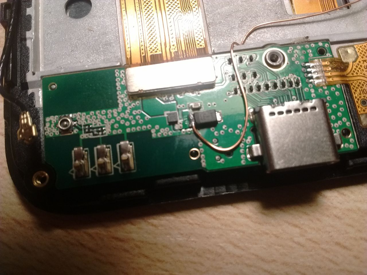
I received a PinePhone that never charged when plugged on USB. Also the phone does not boot when plugged without the battery. I tried: computer, 1A charger, 2A Asus charger, 2.1A battery. On OSes: latest pmOS and Ubuntu Touch, default test software. Apart from that (USB power issue), the phone seems to work correctly. The phone is seen has a "PinePhone" when connected with USB to a Linux computer. See https://forum.pine64.org/showthread.php?tid=9042
Investigations: If I measure VBUS (aka DCIN in older schematics) on the USB-C daughter board connector (using multimeter, touch the leftmost pins on the bottom row, they can be reached even with the flex cable plugged), I get when flex cable unplugged: 4.7V (sometimes 2.3V but less often and not reproducibly), when flex cable plugged: 1.21V (it should be 5V!).
I did measurements using names from "PinePhone USB-C small board schematic v1.0 20190730.pdf" given to me by TL on the Telegram dev chat. I measure C101 to be 3.3 uf instead of 4.7 uf according to schematics. I measure C104 to be 265 pf, C105 to be 0.26nf, C106 to be > 10 uf (my tool does not go above)., C107 to be: 0.18nf.
I decided to bypass OVP to try fixing my PinePhone:
With this bypass, the phone is able to boot with or without the battery, and to charge the battery. As this is a hack that reduces safety I will try to have my USB-C daughter board replaced.
Pogo Pins supply 5v0, not 3v3
This is possibly just a documentation issue. The wiki claims they provide a "3.3v power source", and on this page, "The Pogo Pin specified voltage is 3.3v". But according to the schematic, they are connected to USB-5V, the output of the 5V boost regulator.
ANX7688 power supply situation is suboptimal
ANX7688 has four power inputs: 3v3, 1v8, 1v0, and HDMI_VT (which is also 3v3).
- The main 3v3 input, to AVDD33, should always be on. For this reason, it should be connected to an always-on regulator, such as DCDC1, so DLDO1 can be turned off when the screen is off. It has extremely low power consumption.
- HDMI_VT is only needed during video transmission, and should remain connected to DLDO1.
- The only other 3v3 consumer is the VCONN_EN pull-ups. These could be pulled to GPIO1-LDO (1.8V) instead; the pins are open drain.
- The DVDD18 input should also always be on. It has extremely low power consumption. I recommend connecting it and the PL11 pull-up to VCC-PL, so GPIO1-LDO can be turned off.
- The remaining 1v8 inputs only need to be enabled when a USB cable is connected (supply or OTG). They are connected to their own regulator (GPIO1-LDO), so that is fine. (Note that the next issue suggests removing the pull-ups for POWER_EN and RESET_N.)
- The 1v0 input is only needed when a USB cable is connected (supply or OTG). It is currently controlled by DLDO1, but I think controlling it with GPIO1-LDO would be an improvement. That way DLDO1 only needs to be enabled when transmitting video, not always when a cable is connected.
See https://wiki.pine64.org/index.php/PinePhone/Power_Management#Regulators
ANX7688 power/reset control pulled the wrong way
Both ANX_POWER_EN and ANX_RESET_N have pull-ups when they should not. Both signals need to be pulled low by default. They only need to be brought high (turning the chip on) when a USB cable is attached; and they should only be brought high after the 1v8 and 1v0 regulators are turned on. ANX_POWER_EN needs an external pull-down. ANX_RESET_N has an internal pull-down.
VCONN_EN signals are possibly inverted
I don't have a datasheet for the AW3512 chips, but I assume the enable input is active-high. VCONN1_EN and VCONN2_EN are open-drain. When they are open, it appears that VCONN should be enabled. But right now, when they are open, VCONN is disabled, because the AW3512 EN pin will be pulled low by the FET.
Speaker output could be differential
If a differential connection to the speaker amplifier doesn't cause any issues, using it would significantly lower the noise floor of the speaker, and would allow doubling the max volume.


